|
Designing DigitalHardware Using VHDL |
VHDL stands for ‘Very High Speed Integrated Circuit
Hardware Description Language’
Unlike all other computer languages it’s a substitute for
directly defining the function of any hardware we develop.
Mainly it consists three processes
1. Design
2. Simulation
3. Synthesis
Design :- its a process where we actually
develop skeleton of the hardware we are going to produce. So here our major
task it to define the functionality of the hardware we are designing. Just like
the following AND gate program

library ieee; block 1
use ieee.std_logic_1164.all;

entity yand
is
Port (A,B:in std_logic; block 2
C:out std_logic);
end yand;

architecture behaviour of yand is
C<=A and B; block 3
end behaviour;
As shown in
above code the program is divided into three
blocks.
In this is very simple program where we defined the
functionality of and gate using the statement c<=a and b;
The first block of the program is used to include libraries
where and & all other keywords & data types in VHDL were defined. Just
like #include<stdio.h> in C language.
The second block speaks about an entity which will have
ports defined by the ‘port’ statement i.e. a and b are input ports & c is out
put port which all hold a value of datatype defined by the statement std_logic.
The third block speaks about the actual behaviour of our IC
in design.
C<=A and B may be considered as the heart of the program.
Where the output port C will have the value which is obtained by performing and
operation on the values of A,B.
i.e. if A=1 & B=0 then C will be 0. as per Boolean
algebra!
Ok guys now I am running out of time I’ll write about the
remaining parts next time. Till then you keep practicing VHDL
Those people who want to have a VHDL compiler may download
it from the
Altera site
19-2-2005
Simulation:-
Now we will discuss about simulation. Simulation is a
process where we compile the source code we developed normally these source
files are with *.vhd extension, through any simulation software. The result
obtained through this process will be in the form of wave diagram or truth
table. The example is shown below.
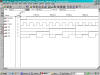
Which is wave diagram for 4-bit upcounter. The design and
simulation processes are repeated until we get desired output.
Simulation:-
Here we are in real business. Our aim at this
stage is to implement the simulated output on to a
FPGA. FPGA stands for Field Programmable
Gate Array.
There are several FPGA kits available for self study.
One of the popular one is spartan series of
Xilinx
.
| 